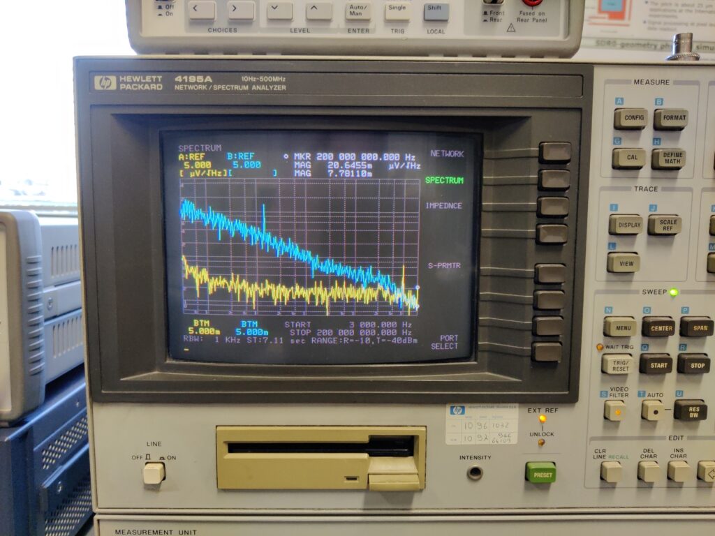
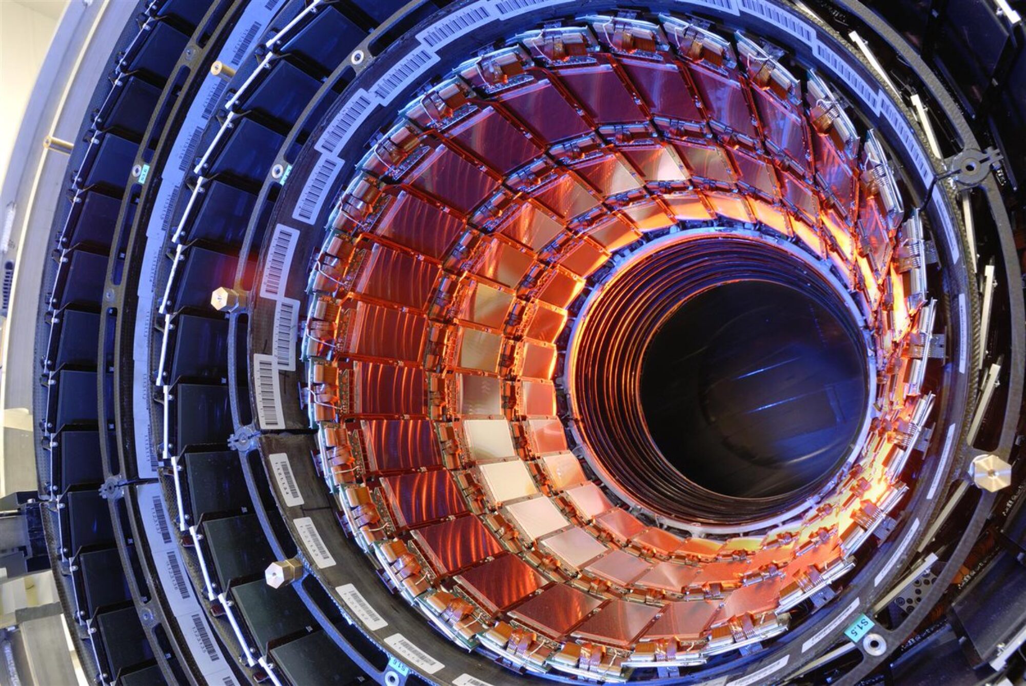
The ARCADIA experiment, funded by INFN, aims at the development of a low power, fully depleted CMOS monolithic sensor for multiple applications, including charged particle tracking in high energy physics and astrophysics experiments, medical imaging and photon science. The 110 nm CMOS process the sensor is based upon is being characterized at the EIL. For this purpose, a test chip has been designed, including both NMOS and PMOS transistors with different width and length. The devices have been characterized from the standpoint of static and signal parameters. Noise measurements, for which a noise amplifying stage has been purposely developed, are now in progress.

